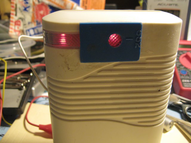
It all started with one of those proximity sensors that detects motion and then transmits a signal to a little box (shown here) that chimes three times and flashes some LED lights three times. The sensor will let me know when someone enters my garage. But I thought---wouldn't it be nice to know if someone was in there when I wasn't home. So the project began of how to make the chime box record a date and time. I decided to feed it into my computer somehow. So I started here by gluing a small piece of plastic, with a hole in it, over one of the LED lights.
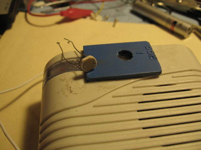
Next I selected a photo resistor that would just fit in
the hole. I would use this to do what is called an "opti-coupler"
This is coupling the next circuit through the use of "optics." The LED
will flash---and the photo resistor will pick it up. Since photo resistors
vary in resistance---according to the light hitting them---then I would need to
build a circuit that would detect that light and in doing so close a relay to
activate the next circuit.

Here is the photo resistor placed in the hole and up
against the lens for the LED light. I will mix up a batch of J.B.Weld
epoxy and use it to hold the photo resistor in and to also cover the rest of the
LED lens so as to block any daylight from reaching the photo resistor.
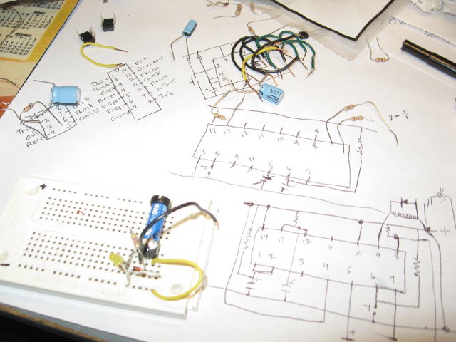
Here I learned to design a circuit for the photo
resistor. The schematic will follow. I always assembly everything on
a test "breadboard" before committing to building it on a printed
circuit board. There is a potentiometer on the right to adjust the
sensitivity so that the LED light on the circuit board---along with the
relay---will activate when the photo resistor senses the light from the
receiver's LEDs in the chime box. Ok---this is working like it
should. But there is a problem. The chime box flashes the light
three times. Hence the photo resistor will pick it up and close the relay
three times. Since I want to send only ONE signal for the alarm---I need
to have a circuit that will do that. The next circuit will do
that.
I want the final single signal to be an input for a key
on the keyboard that feeds into a computer. So I was going to build what
is called a "one shot monostable timer" This uses the 555 timer
chip. In this case---since it takes 5 seconds for the chime box to flash
the lights three times---I made a timer that is triggered by the first flash and
then runs for 6 seconds. This means the second and third flash have no
affect on it. Hence we now pass on a single signal out for three signals
in. But now another problem. This is producing a 6 second
signal. Have you ever held a key down for six seconds. If you
have---then you know it makes hundreds of entries instead of just one. So
that is why you see TWO 555 timer chips. One is set up to receive a signal
from the photo resistor and run for 6 seconds. Then it triggers the next
timer that runs for about 1/10 of a second. This will produce the 1/10 of
a second input to the keyboard.
In an effort to make things smaller, I decided to use a
556 chip. That is two 555's in one chip. Here you can see that I
designed what I needed to do. I should add that when I say I "design" I
mean that I figure out how I am going to wire things and the final layout of
what I am building. Since I am just reuniting myself with electronics
(having not dabbled in it for many many years) a great deal of my
designing is built on other people's schematics and ideas. I am finding
there is a vast world of people sharing such projects. Hence I am
publishing mine in hopes of inspiring others as I have been inspire. The
schematic for this will follow.
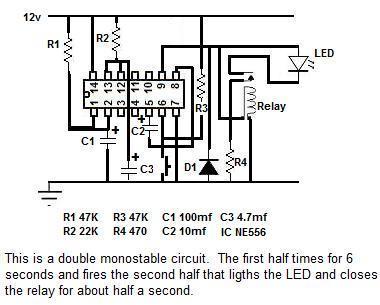
This is what I designed for the 556 chip but in this example it's second pulse was 1/2 a second. I found later I wanted it lower to about 1/10 so changed the values on the second resistor and capacitor set. The drawing is very hard to follow for others. Since I designed it I knew what I had drawn. I may do it over some time. If anyone would really be interested in more info ---and I get around to putting an e-mail link---you can write me with your questions. But for now---this is more of an "inspiration" page than a real "How to do it." page.
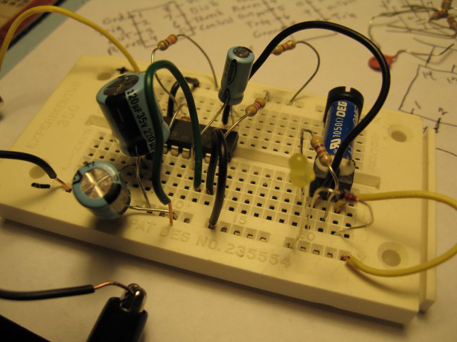
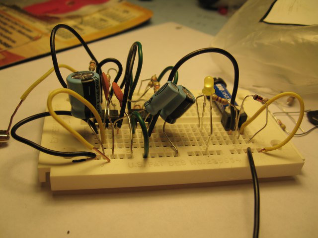
So here id the breadboard circuit using the 556. Everything is working
fine and it can now be transferred to a more final printed circuit board.
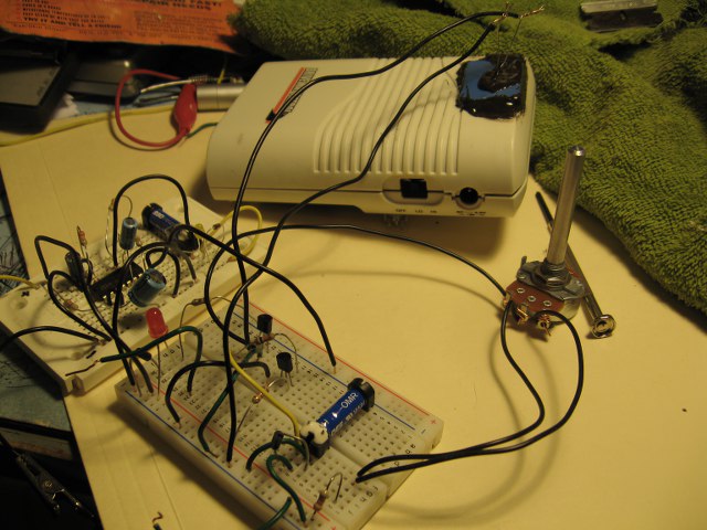
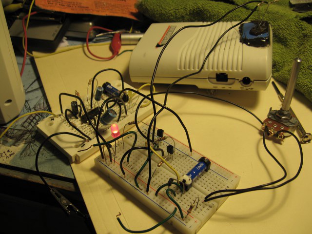
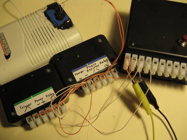
Here is the chime box and the opti-coupler and the 556
all linked together and being tested. Again---everything is working fine
and it's time for the next step.
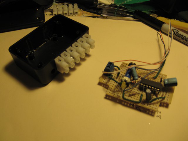
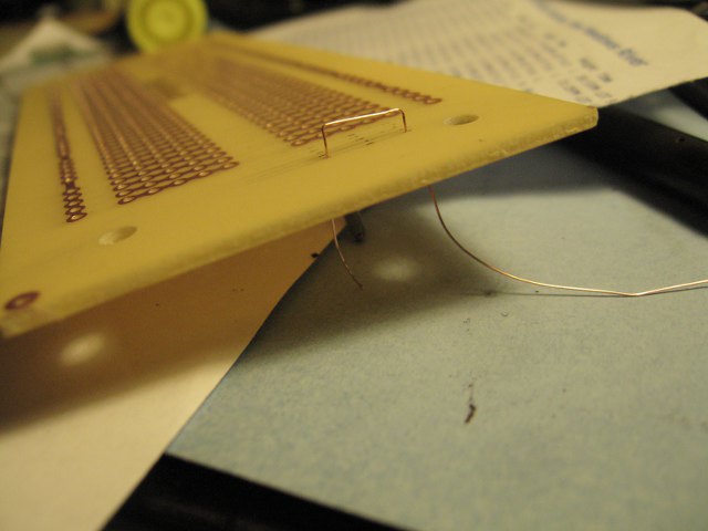
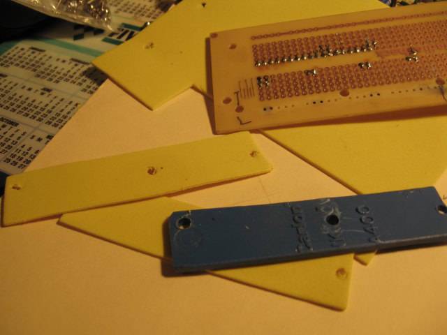
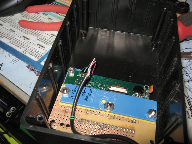
This is the 556 committed to a printed circuit
board. I wanted it in a small box and decided to put outside terminals in case some day I wanted to use this in another circuit
combination The large potentiometer was of course replaced with a small
circuit board one. The board itself was a bit to big for the box so I
ground off all four corners and drilled some holes in it to mount it to the
small plastic posts at the bottom of the box.
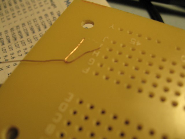
Here it is---fitting nicely in the box and with all of it's important
connections coming out to the terminals. There are the battery
connections---and two for the photo resistor--and finally two that are closed
by the relay. These don't feed the relay---they are the normally
open contacts that close when it is powered.
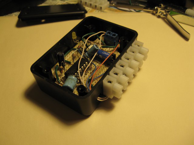
In this picture you see that it is the opti-coupler circuit that has been put on
a pc board and installed in another small box. This has two terminals for
power---and two for it's own relay -----and two to trigger it. There is a
small LED light that will protrude up through the cover and light up when the
circuit's relay has been activated. I thought it a good idea to have
most all the relays monitored. This way if some part of the circuit fails
I will have a visual idea of where it might be at by the unlit LED.
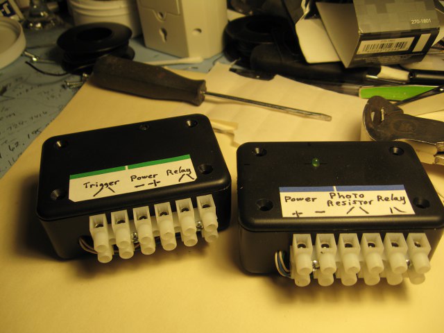
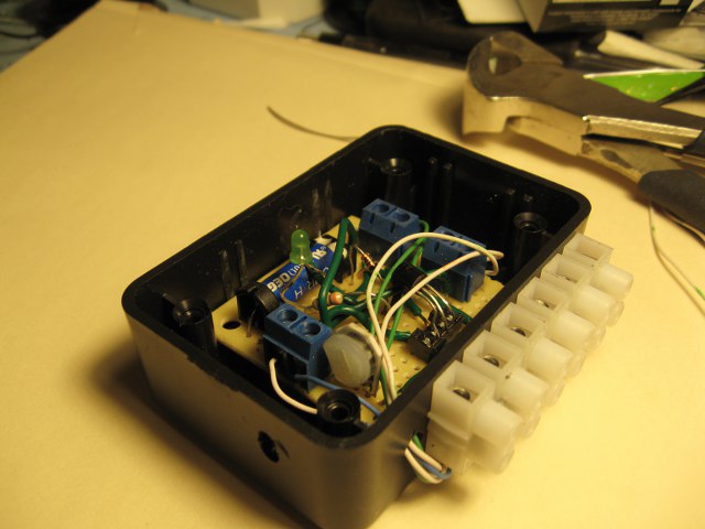
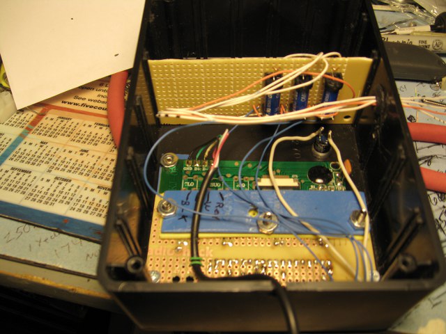
Now the two boxes are finished. When they are wired up the photo
resistor will be wired into the opt-coupler where it says---of course---:photo
resistor." Then two wires will go from the opt-coupler's relay output to
the "trigger" input on the monostable timer. The relay output on the
monostable timer will then send the 1/10 second pulse to the next stage..
Now for the next step----getting the 1/10 second pulse into the computer.
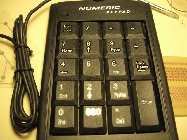
I have a program on my computer that recognizes numbers coming from the
numerical keypad on your keyboard. That's the numbers on the right that
you usually turn on and off with your "Number Lock" key. The program only
recognizes the "numerical keypad" part. So I can type in regular keyboard
numbers and nothing happens. But when coming from the numbers on the
right---the software program will recognize them. But I didn't want to
tear my keyboard apart to do this. So when I discovered this numerical
keypads that you can buy separately---they were just what I wanted. It
plugs into the USB port. Now I had something to tear apart.
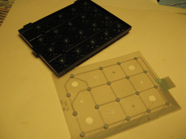
Once the keypad is torn apart there is a small circuit board with a
microchip that feeds into the computer. This picture doesn't show the
board and chip---but you will see it later. This shows how the keypad
feeds the chip. the keys push down on this double layer of plastic that
has little trails of a graphite material etched onto them that acts like little
wires. When you push a key down you are really are squeezing
together two contacts and shorting two parts of the circuit together.
Basically there are 9 wires that feed the chip. By touching different ones
together you create numbers 0-9 plus a few other commands. So my plan is
to have 9 little relays that will short the correct contacts together to
get numbers 1-9.
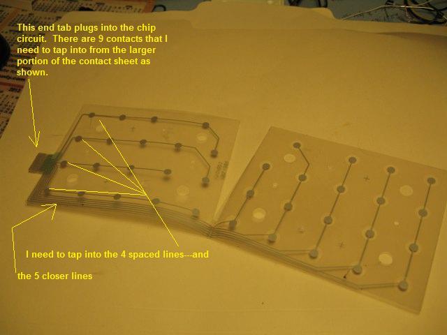
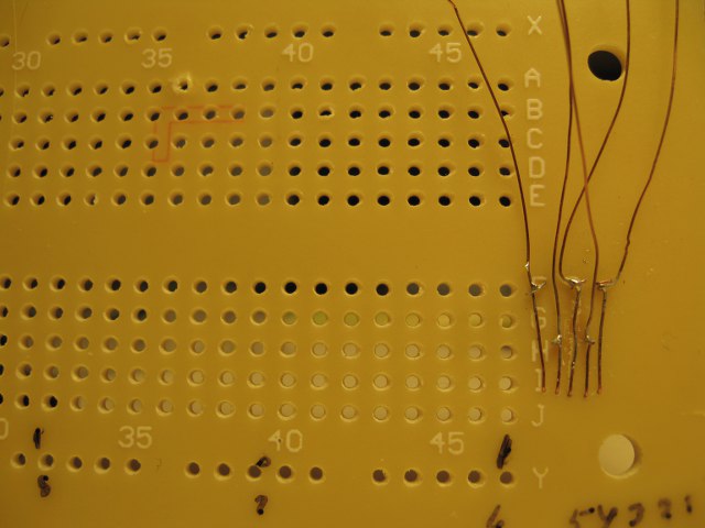
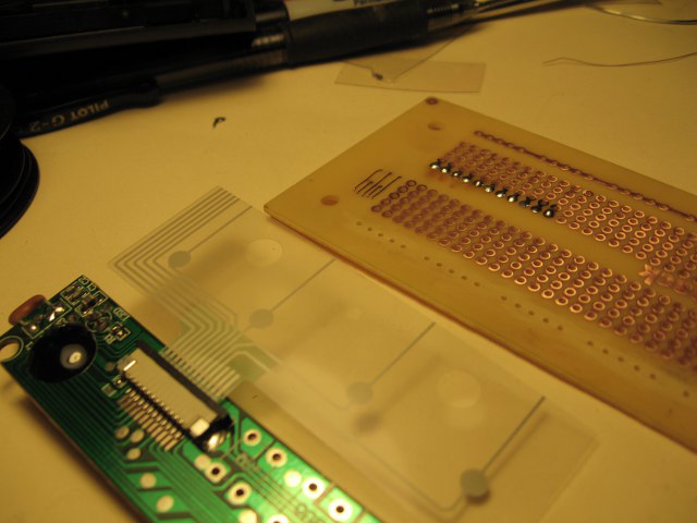
With the etched plastic opened up you can see how the 9 original circuits
that show on the small tab to the right---weave around on the plastic in
such a way that when it is folded back together some contacts from one circuit
are hovering over contacts from another circuit ad just waiting for a key to
push them together. I was originally going to try to solder 9
wires onto the chip board. But you will see it later and see why it was
just too small for me to be able to solder. So I wanted to figure a way to
get this contact plastic to transfer it's signal to a pc board. If you
look closely you'll see the little tab has the 9 contacts that plug into the
chip. From there they lead down the plastic with 5 of them on the outside
and 4 are dots across the top of the plastic. I needed to find some way to
press these against a copper pc board and transfer the signals. You can
click on the picture for a larger one.
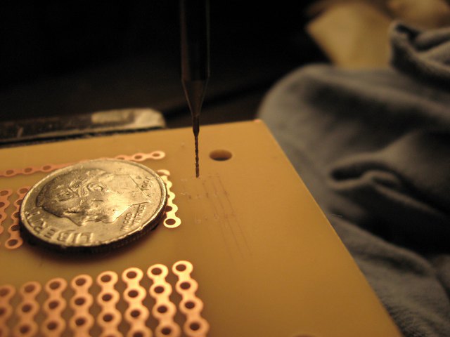
I started out with a generic pc board from Radio Shack. Remember I
said there were 4 round dots that would hit this board. those are the easy
part. But the 5 lines coming down the outside of the plastic are the hard
ones. They are very close together. I would have to make some
contacts for them to hit. So I started with a 1/64s drill bit. Note
the dime for comparison. These things are like hair fine. They break if
you look at them wrong. So they definitely had to be mounted in a drill
press to be kept steady while drilling. I had to be very careful and take
the time to watch closely before advancing the bit. To much pressure and
they would snap too. But I finally got 10 holes drilled. 3
sets were further apart than the other two sets. You will see why later.
I took a piece of stranded wire and stripped it to get the inner
strands. they look big here but were really small---as they fit through
the 1/64th holes.
The wire is pushed up to the copper side of the board.
Sharp bends are made in the wire so that it can feed up through one
hole---lay very flat on the board---and feed back down through another hole.
On the back side the wire is gently twisted around itself and a drop of
solder is added to hold it tight. Remember I said 3 sets of the holes were
further apart than the other two sets? Well the reason for that will show
in the next picture.
The sets are all finished and soldered with their extra leads read to feed
off to another part of the board. Not the solder joints are
staggered. They never would have been able to be all at the top or they
would have bumped into each other. Hence why some of the sets are shorter
and some are longer---to stagger the soldering joints.
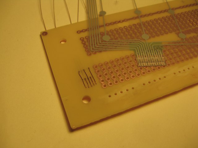
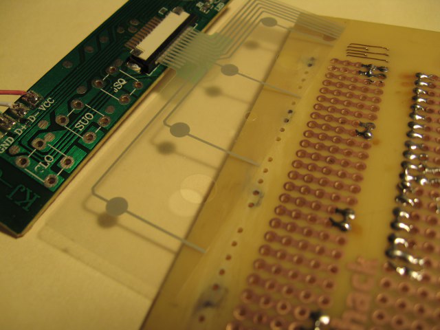
Now you can better see how the plastic contact sheet is going to mesh with
the pc board. The tab with the 9 contacts will come towards you and plug
into the chip board that you will see in pictures below. Then the 5 lines
on the left of the sheet will mesh with the 5 wires I installed on the
board. You will also see 4 dots from the other 4 circuits. Those
will fall on random contacts already on the pc board. In the end I will
have access to all 9 inputs to the chip.
I decided to trim of some extra length to the plastic so that I had just
the 5 outside leads and only one row of the 4 dots. things are lining up
nicely now.
Now I take the time to extend the leads from the 5 wire contacts that I
made. I flip the board over to work on them. I extend them to
contacts further up the board so as to have a place to solder to later and not
have to disturb these 5 spots again. Because they are bare wires I slip a
little insulation over each one and make sure they don't touch as I stretch them
to solder them above. Once all is done a put a tad of hot glue on them to
hold everything in place.

Here is the board flipped back over. I took each of the five wires
and brought them up through one hole and down through the adjacent hole.
this way I have two rows of contacts to solder to---for each wire. I
probably won't need that many---but figured I'd do it while I had the chance.
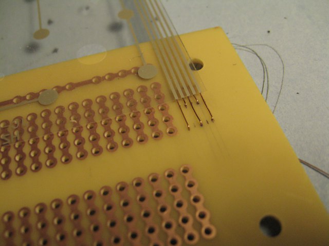
Now you get to see the chip board from the keypad. The chip is buried
under that round circle of epoxy. The tab with the 9 contacts fits into a
little plug that then has a wedge pushed in to jamb it against the contacts that
lead to the chip. You can click on the picture to enlarge it. You
will see how close together the contacts are. I didn't dare disturb their
solder for fear of making a mess of it all. Hence the reason to find a
more "mechanical" way to join the chip to my relays. Hence all this work
to make the pc board with the contacts.
Note in this picture I have determined where the 4 dots will hit the pc
bard and have extended there row of contacts to the contacts above. Hence
there are 4 solder joints on the left, where the dots will hit, that lead to 4
"sets of 2" contacts above to go with the 5 "sets of 2" already there. I
now have my 9 sets of access to the chip.
The time is taken to slide the board sideways until it matches up with the
5 home made contacts I built. I put a small piece of plastic and hot glued
it to hold things in place.
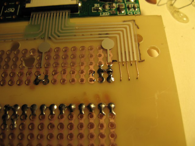
The board is flipped over and everything is lining up. Phew!!
I got some thin pieces of foam from the Dollar Store, in their craft area,
and cut some strips to match a piece of plastic. The plastic was cut to
bolt to the pc board and compress the plastic circuit sheet against the circuit
board's copper contacts.
To make sure the plastic sheet is being pressed against the pc board copper
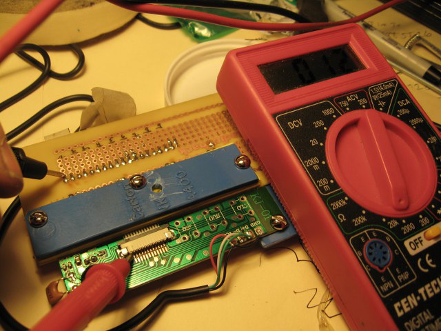
contacts----I check each circuit for continuity. All is well..
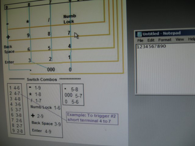
This is a picture of my computer screen. On it is an open picture I
made of the keypad and what wires needed to be shorted together to get what
numbers and symbols. I opened a Notepad beside it and began shorting wires
that would make 1-0. As you can see---they all worked.
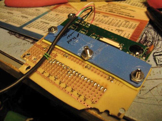
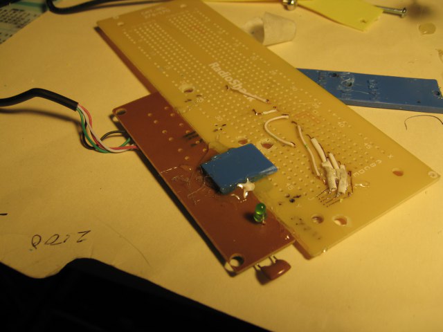
Now to mount things together. Here everything is checked over and the USB
wire is tied to the board so as not to tug on the ends that are soldered.

The back side is checked. And extra piece of plastic was bolted to
hold the chip board to the pc board. The glue was working ok---but I
wanted an even better and tighter mechanical bond.
The board is again flipped over and placed into a larger project box so
that the little green light ---on the circuit board---will poke through a hole
on the back of the box. This is the light that tells when the numeric pad
has been activated. Later I will add a push button switch---near the
light---to switch the keypad on and off.
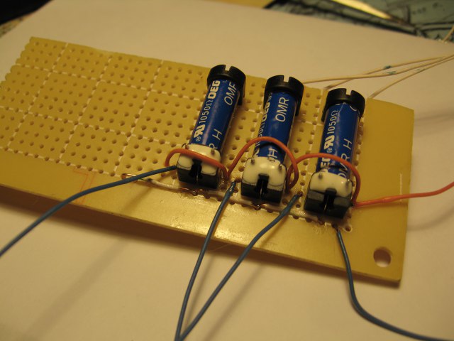
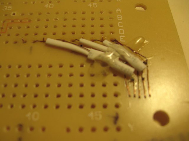
I stared with only 3 relays at first. I will need nine for nine
numbers. But since I only have one alarm built---I really only need one
number now. I just added two more for later. I started to mess up
this wiring---so pay no attention to it. In the end there will need to be
two wires in to power EACH relay---which in turn will short tow wires that
activate the number it is meant to represent. For now I will wire one
relay to activate #1.
The board is slid into the slots above the main board. It has already
been wired to the main board.
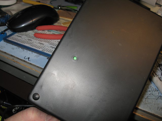
The cover is put on the box and it is flipped over to show the small light
that will be on when the keypad is active. A switch is added later and
shows up in the picture below.
Here are all the circuits linked together. I probably could have put
them all on one box if I had designed things better. But the bottom line
is that it does what I want. Hopefully I will get better at planning these
things. there was already a lot that I did that could have been
worse. I'm pleased with the results.
What stared out as a simple idea got rather complicated. And I'm sure there may have been other things I could have done to make it simpler. I don't like a lot of mechanical relays and should learn more about transistor switching etc. But for now it works. And what does it do you ask.;-) Well if someone enters my garage it starts the remote chime flashing the LED lights. The opti-coupler picks up on the lights and activates the first half of a 556 timer for 6 seconds. The timer then triggers the other half for 1/10 of a second. That 1/10 of a second signal is sent to the computer via the hacked keypad. The program in the computer recognizes the number and runs a dos batch file. The dos batch file opens a wav file that says.. "Garage security has been activated" At the same time it announces the wav file it opens a Notepad log book and enters the time and date.
There you have it. I can come home and see if anyone has been in my garage besides me. I can turn the sound on when I want to hear the wav file---or turn it off when I don't want others to hear it. If I don't activate the keypad box with a switch---then the alarms are not set and nothing gets announced or logged in.